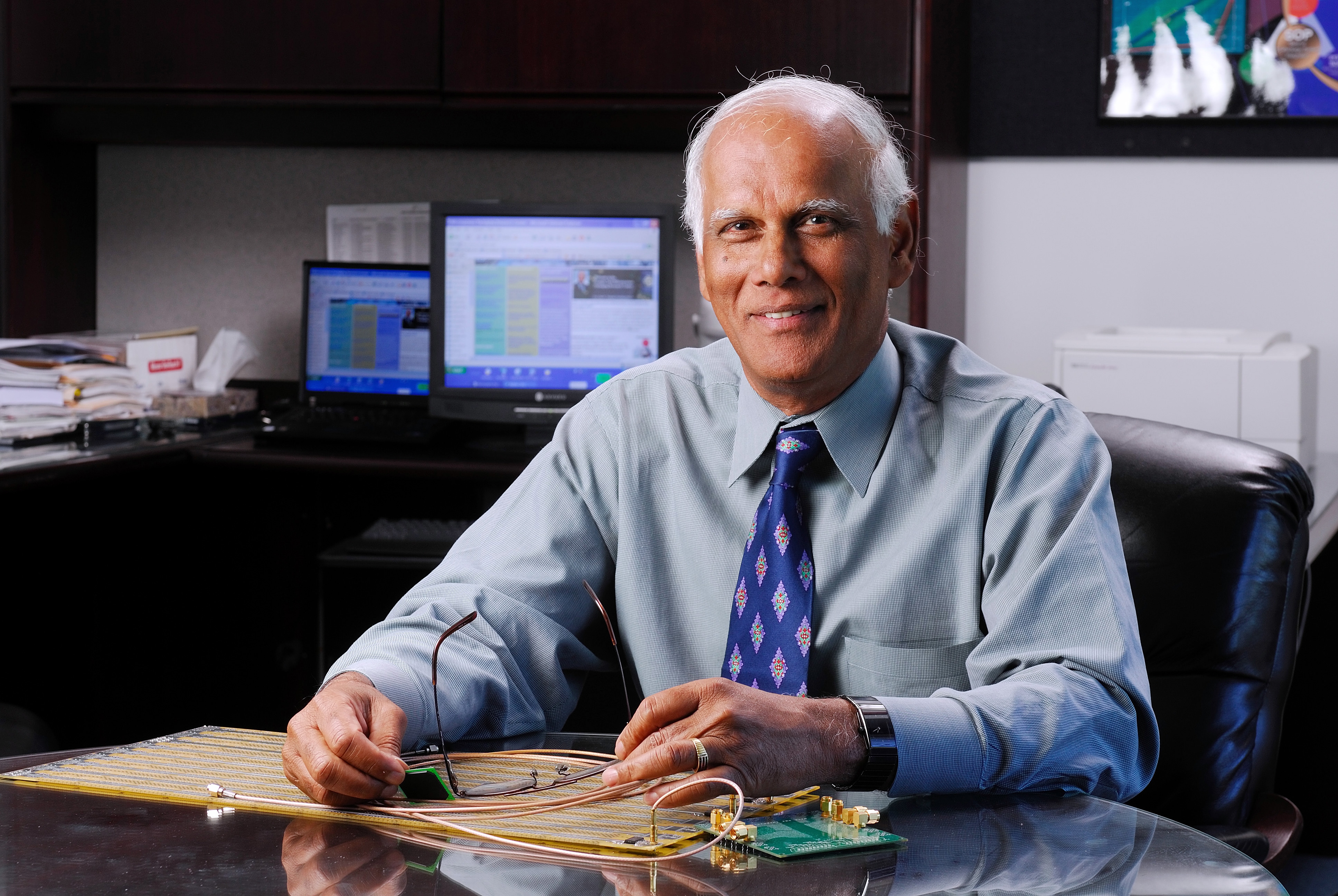
Prof. Rao R. Tummala
General Chair & Organizer, IDSPS 2026
A globally renowned pioneer in microelectronics packaging and integrated systems — with over 800 technical publications, 110+ patents, and seven authoritative textbooks. Elected to the National Academy of Engineering in both the USA and India, and widely regarded as the "Father of Modern Electronic Packaging".
Emeritus Professor, Georgia Tech
Father of Modern Packaging (IEEE)
Advisor, Indian Semiconductor Mission
Education & Early Career
Academic & Professional Journey
- Born in India; graduated from Andhra Loyola College and the Indian Institute of Science.
- Pursued his Ph.D. at the University of Illinois.
- Joined IBM, rising to the prestigious rank of IBM Fellow — the company's highest technical honor, awarded to roughly one in ten thousand employees.
- Served as Director of the Advanced Packaging Technology Lab at IBM Research, shaping IBM's global strategy in advanced packaging technologies.
- Joined Georgia Institute of Technology to establish the Packaging Research Center (PRC) as a National Science Foundation Engineering Research Center (NSF ERC) — one of the world's largest and most successful industry co-development centers.
- Pioneered the System-on-Package (SOP) vision, anticipating the shift from on-chip integration to on-package system integration.
Pioneering Contributions
Key Innovations
- Developed the industry's first plasma display technology in the 1970s.
- Designed one of the first large-scale 144-chip, 127 mm multi-chip packages for servers, mainframes, and supercomputers in the 1980s.
- Invented the first Low Temperature Co-fired Ceramic (LTCC) technology, revolutionizing RF and wireless systems — particularly in defense and space applications.
- Pioneered the System-on-Package (SOP) concept to address the slowdown of Moore's Law.
- At Georgia Tech, introduced the Industry Co-Development Center model, partnering with global companies to advance next-generation packaging technologies.
- Led pioneering work on glass panel packaging — a leading-edge technology for AI and high-performance computing, beyond traditional silicon interposers.
- Invented six major technology products and authored seven influential textbooks in microelectronics packaging.
Educational & Industry Impact
Impact & Legacy
- Founded the first and largest industry co-development NSF ERC center in electronic systems packaging.
- Led collaborations involving 30+ faculty, 200+ graduate students, and 50–100 global companies.
- Educated 10,000+ packaging engineers and graduated 1,000+ Ph.D. and M.S. students.
- Published 800+ technical papers and holds 110+ patents.
- Authored landmark textbooks, including:
- Microelectronics Packaging Handbook (1988)
- Fundamentals of Microsystem Packaging (2001)
- Introduction to System-on-Package (2006)
Honors & Recognition
Awards & Fellowships
- Recipient of 50+ prestigious industry and academic awards.
- Honored with the IEEE David Sarnoff Award and the ASM International Engineering Materials Achievement Award.
- Named among the "50 Stars in the U.S. for U.S. Competitiveness" by U.S. News & World Report (1999).
- The IEEE Rao Tummala Electronics Packaging Award was established in his honor — recognizing his pioneering contributions as the father of modern electronic packaging.
- Member of the National Academy of Engineering (USA) and the National Academy of Engineering (India).
- Fellow of IEEE, IMAPS, and the American Ceramic Society.
- Distinguished Alumnus of Indian Institute of Science and University of Illinois, and Distinguished Professor at Georgia Tech.
Advisor to India's Semiconductor Mission
India & IDSPS Initiative
- Currently serves as an Advisor to the Indian Semiconductor Mission (ISM).
- Leading the IDSPS initiative to position India at the forefront of global R&D in AI hardware, semiconductors, and advanced packaging technologies.
800+
Technical Publications
110+
Patents
7
Authoritative Textbooks
1,000+
Graduate Students Mentored
50+
Awards & Honours